BUILD YOUR OWN MODULAR
Back to main to BYOM pageDETAILED PSU ASSEMBLY INSTRUCTIONS
This page is dedicated to detailed photographic step-by-step instructions for the assembly of the PSU module in the BYOM kit. It is not necessary to follow the order of these steps, but I recommend doing it if you are just starting out as I attempt to do it in the easiest order. Take your time, a small mistake can sometimes cause hours of debugging! If it is not working, take a break and then come back and check again.
BILL OF MATERIALS
Here are the bill of materials for this module, they should be obtained from the main bill of materials that is printed in the book and on the root page of BYOM website. It is better to use the tick box sheet provided in the book whilst going along, but it is provided here as extra reference. Essentially the reference’s refer to the printed component locations on the board. The book contains images and descriptions of each component so use that if you are not familiar to what part the value is referring to.
| Reference | Value | Qty |
|---|---|---|
| C1, C2, C4, C5 | 100μF 5mm Electrolytic capacitor | 4 |
| C3 | 220pF 5mm Ceramic capacitor | 1 |
| R1 | 1Ω 1/4W resistor | 1 |
| R2,R3,R5,R6,R7 | 1.5kΩ 1/4W resistor | 5 |
| R4 | 10kΩ 1/4W resistor | 1 |
| F1, F2 | Polyfuse 300mA Trip | 2 |
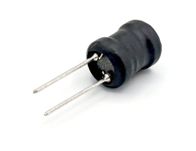
| L1 | 220μH power inductor | 1 |
| D1, D2 | 1N5817 DO-41 diode | 2 |
| U1 | MC34063 IC | 1 |
| U1 Socket | DIP 8 Socket | 1 |
| LED1, LED2 | LED 2mm Red | 2 |
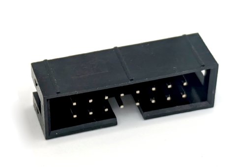
| J5, J6 | IDC socket 16 pin | 2 |
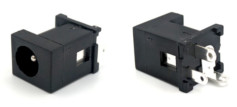
| J4 | Korean Hroparts Elec DC-012A-20A DC socket | 1 |
| Pillars | M3 x 10mm Pillar | 4 |
| M3 Bolts | M3 x 6mm bolt | 4 |
ASSEMBLY
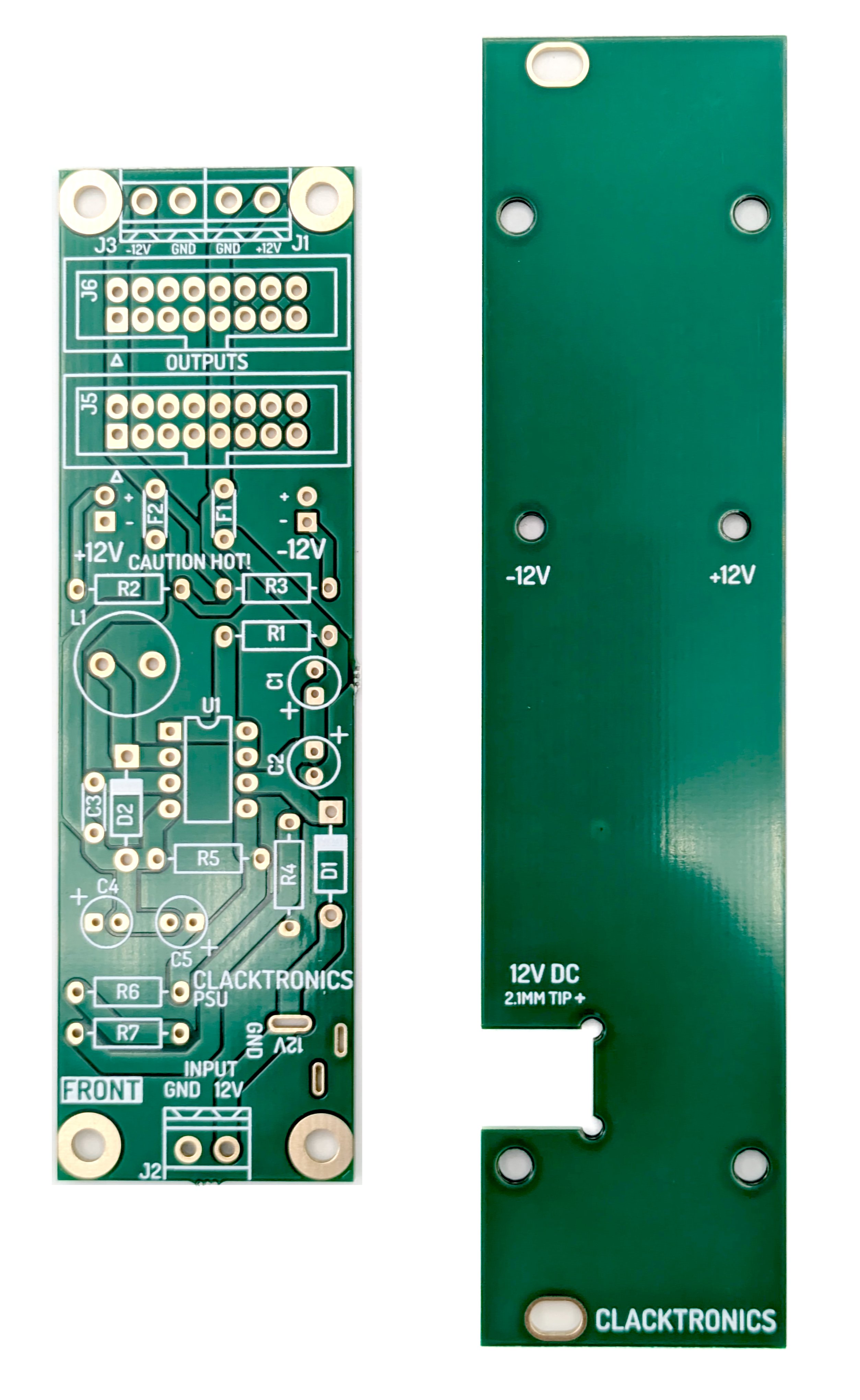
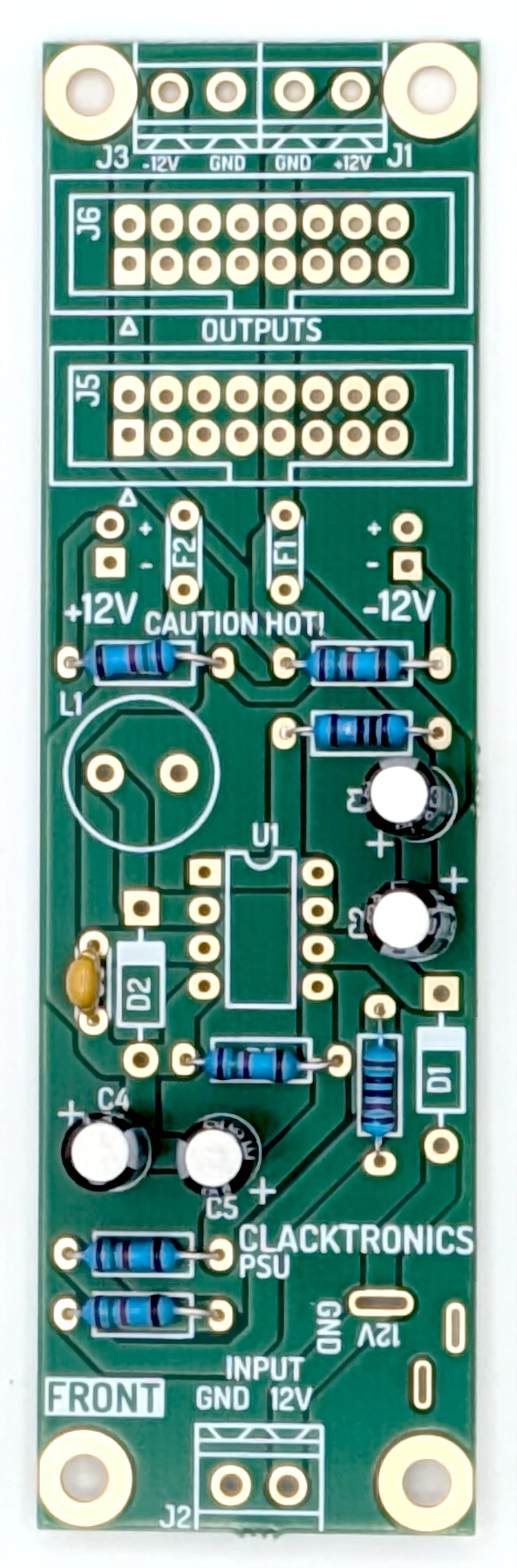
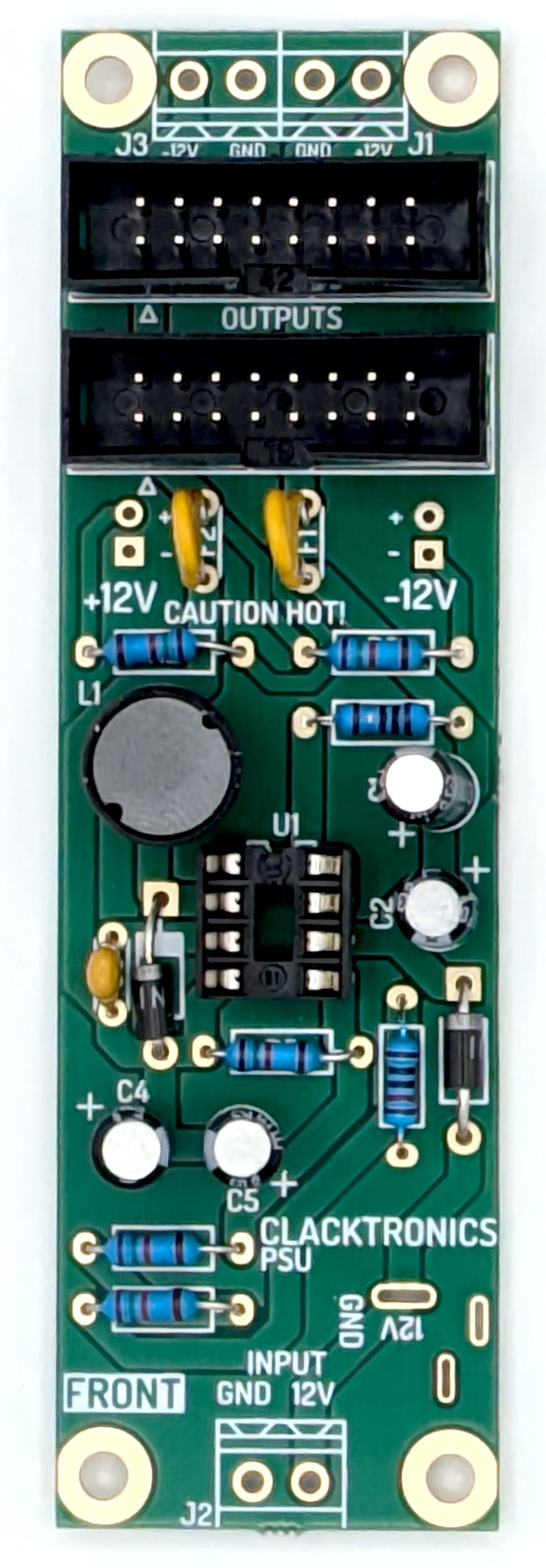
You must start with the two PSU PCBs, the front panel and the main PCB as pictured.
STEP 1 : RESISTORS
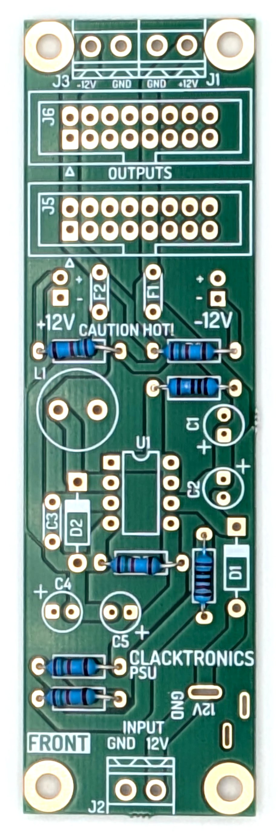
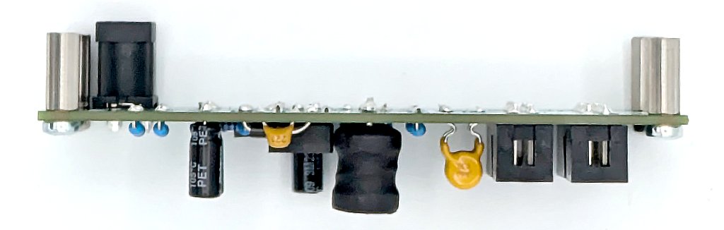
Install the resistors first, as these components can be in some awkward places after connectors have gone on. Make sure you are installing on the "FRONT" mark side of the board. Bend the leads of the resistors as tight as you can up to 90 degrees as they will only just fit in, this was to save space on the board. There are three different values, take care to select the right one, note that 1ohm has a silver band indicator.


Above are the three values needed, use the BOM within the book and tick off the resistors as you go along. Note the way the resistors look can vary quite a lot. There is no orientation to the resistors, they can go either way around, be sure to be installing them on the "FRONT" side of the panel.
STEP 2 : CAPACITORS
There is one multilayer caramic capacitor (MLCC) and 5 Electrolytic capacitors. Ceramic caps fit in either way around, I like to try and keep their value visible from the side so face them outwards. They should be marked with 221 which means 220 pico farads, equals 220pF aka 0.22nF. Your capacitor may be marked different.
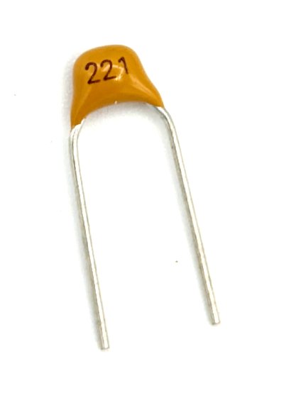
Note your capacitor may be a different colour, or marking than this capacitor as there is variation between different manufacturers. If you ordered them yourself, check the manufacturers datasheet.
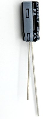
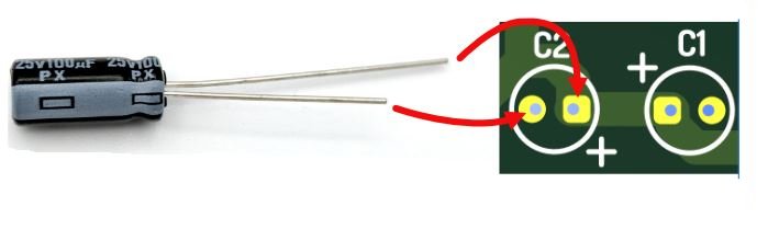
The electrolytics are polarized, they only go in one way around otherwise they are damaged. The PCB is marked with a positive (+), the component is marked with a (-) for negative. The long leg indicates (+) and the short (-). If unsure look at the pad, square pad means (+). You can read the value of the capacitor by reading the text on its side, it is usually in microfarads. In this case 100uF.
STEP 3 : DIODES
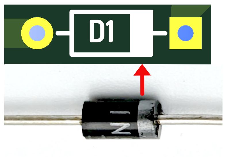
It is essential to watch orientation on these parts. Turn to the component orentation part of the ring binder for a visual representation of how the diode fits the footprint. Bend the leads down slightly wider than we are doing the resistors, these footprints are bigger because the leads on the component are quite chunky.
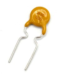
STEP 4 : FUSES
Polyfuses look a lot like ceramic capacitors but they are nothing like them, they are like a resistor that goes very high resistance when too much current passes through them. There are only two to install and they have no specific orientation
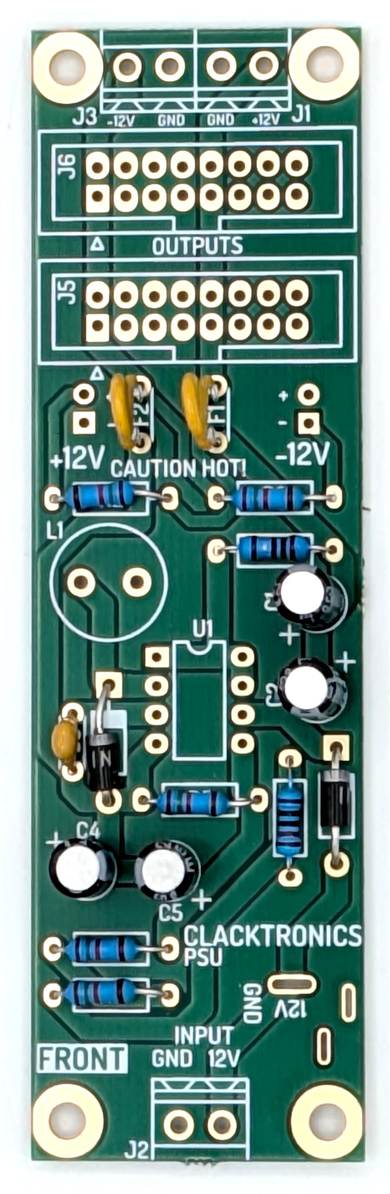
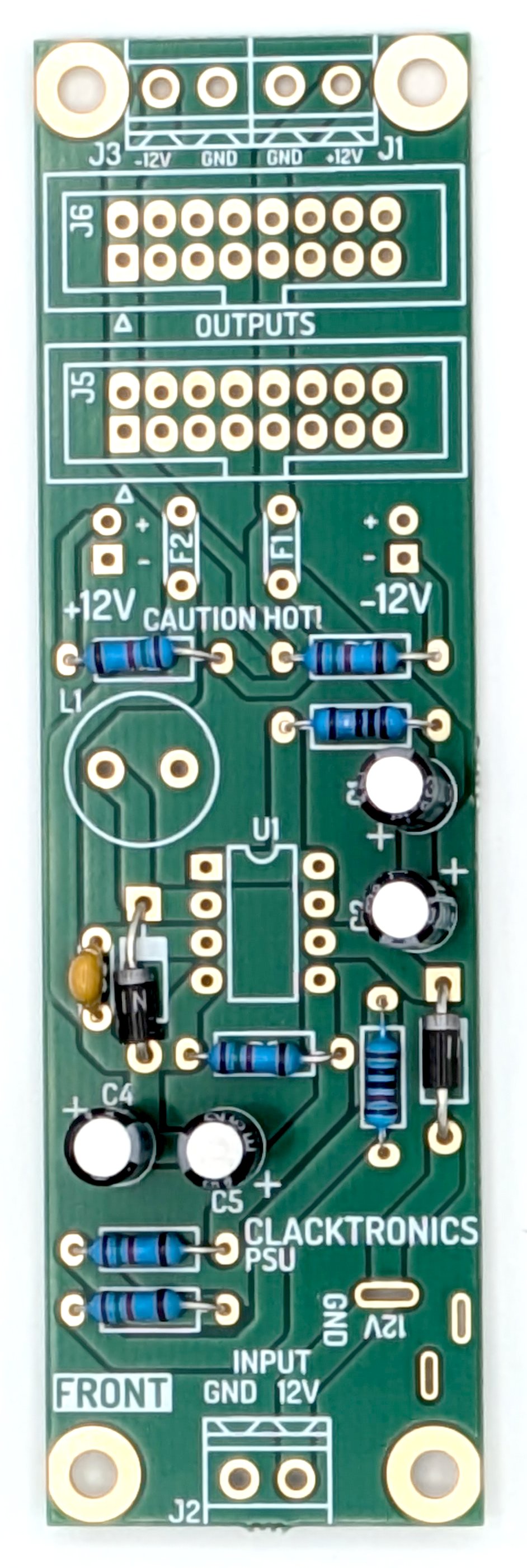
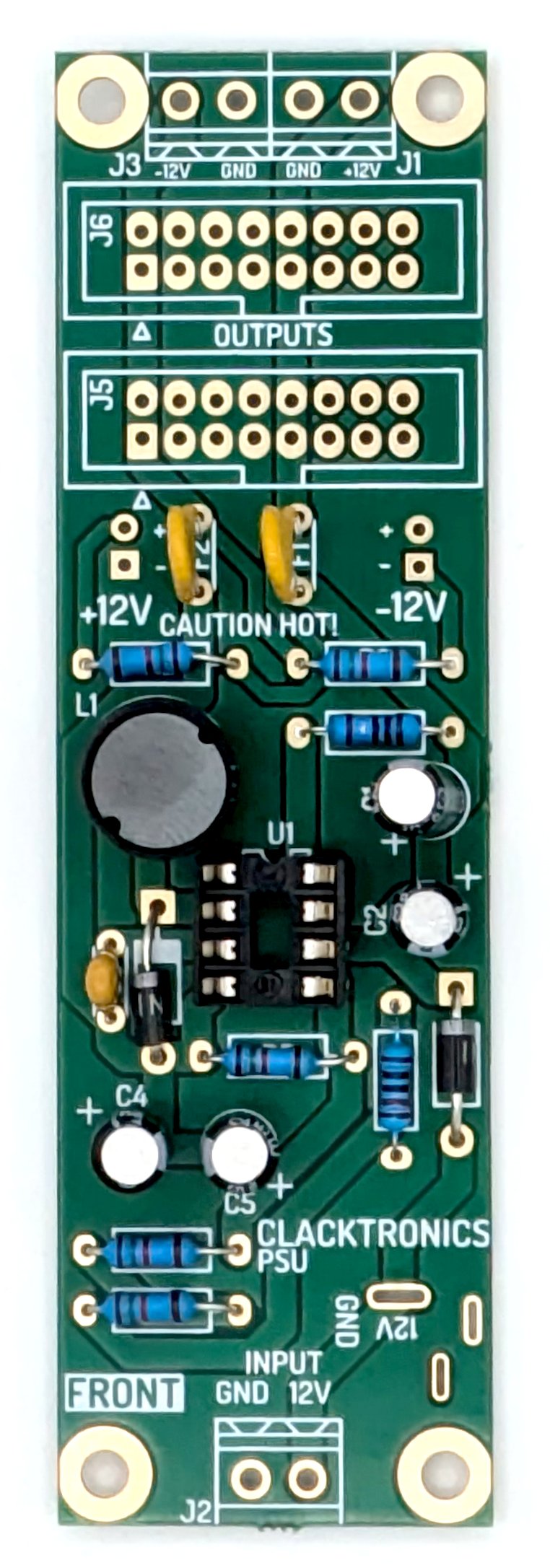
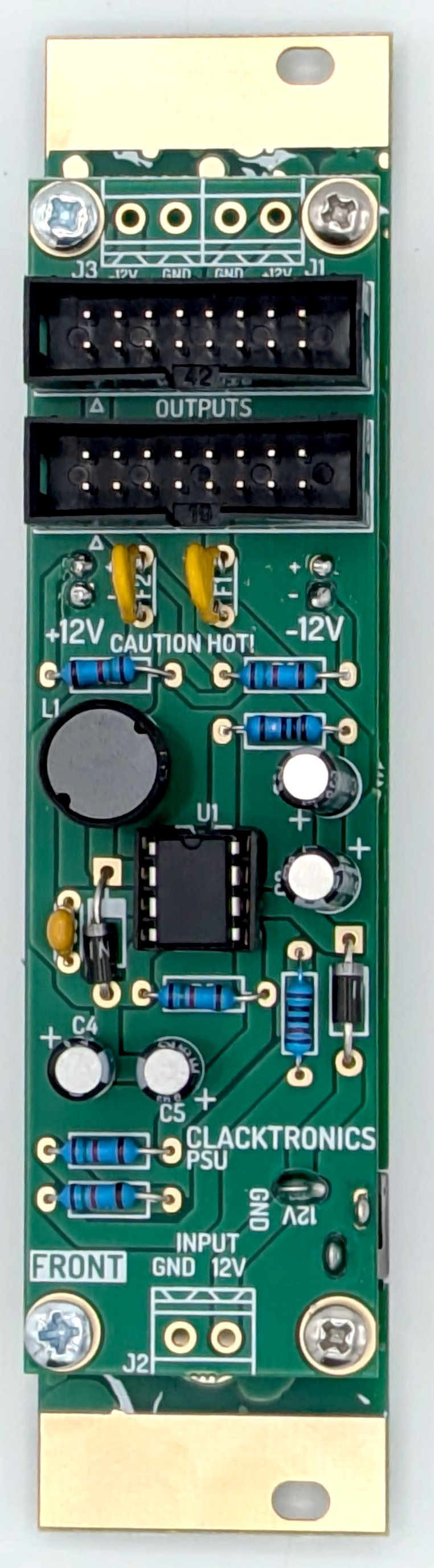
STEP 5 : IC SOCKET AND INDUCTOR
Make sure the oritentation is correct. To solder the IC socket (U1), bend the pins out a little so it grips after installing so you don't have to hold it down when soldering.
The inductor is completely unmarked usually, you just have to know it is the right one. In the kit there is only one so it is hard to get confused. There is no polarity, put it in either way around.
STEP 6 : IDC SOCKETS
For The IDC socket you can't bend the pins because they are short and thick, instead hold in in the PCB and tack a pin at each end, then inspect to see if it is in properly, then solder all the pins. IDC sockets are also orientated only one way around, refer to the orientation section of the book.
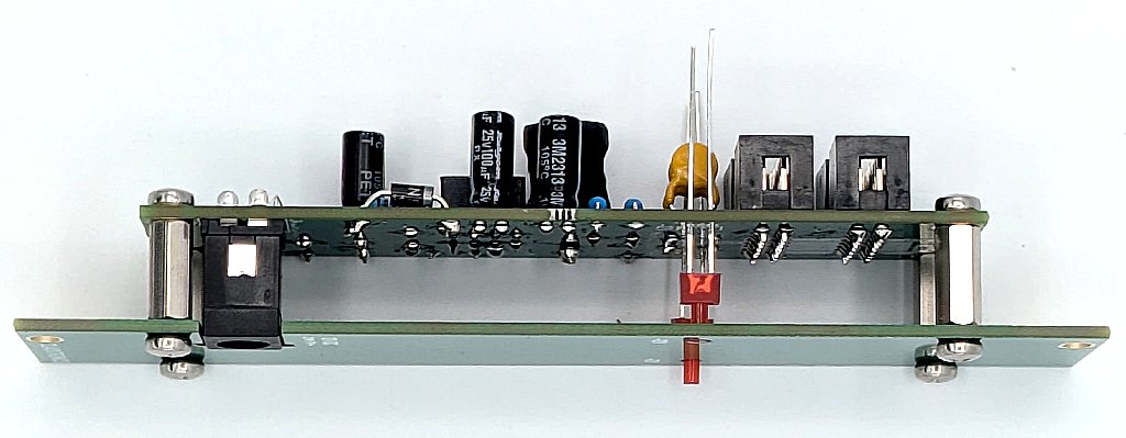
STEP 7 : FLIP OVER AND FIT DC JACK
Everything so far has been on the "FRONT", now we have to flip it over and fit DC jack. It should fit into their sockets snugly and hold itself, so you do not need to hold them down to solder. Feed plenty of solder onto the large mounting pads make sure you fully bury the connectors in solder as this needs to be quite strong.
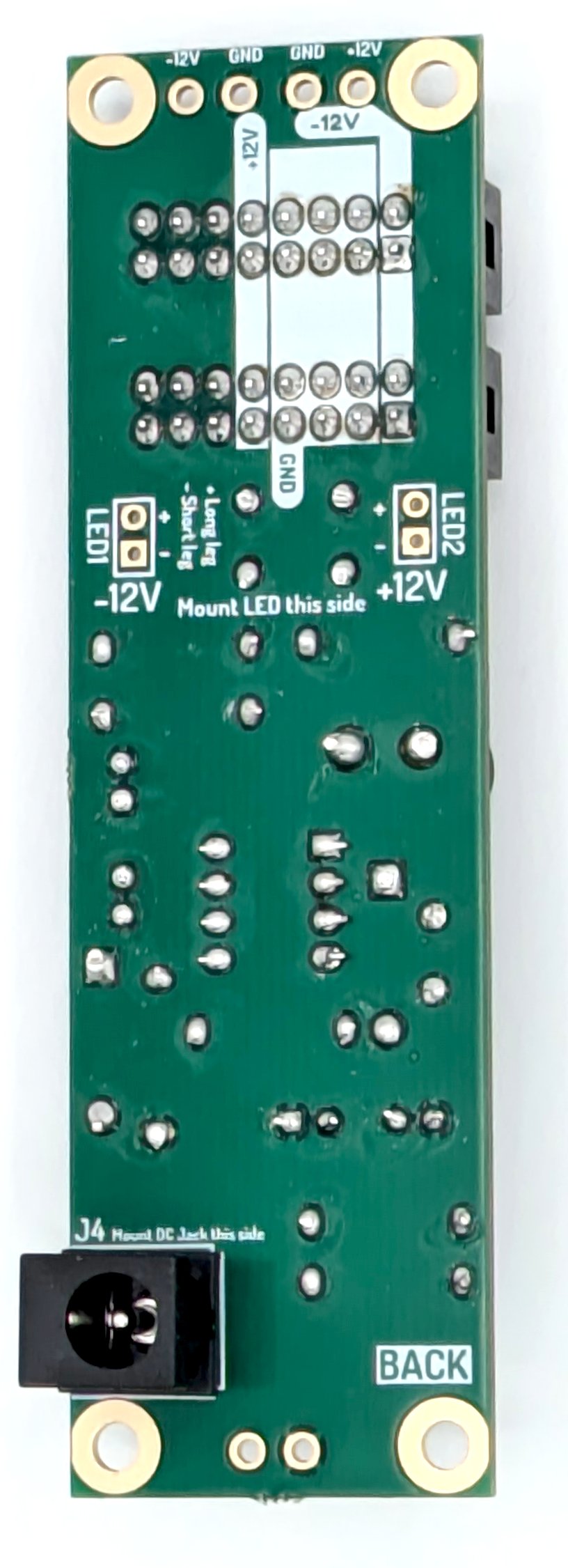
STEP 8 : PCB PILLARS
This module has no components that hold the board onto the panel, instead we use PCB pillars that have the same height as the DC jack. Simply screw them into the board at the corners as pictured with M3x6mm Screws.
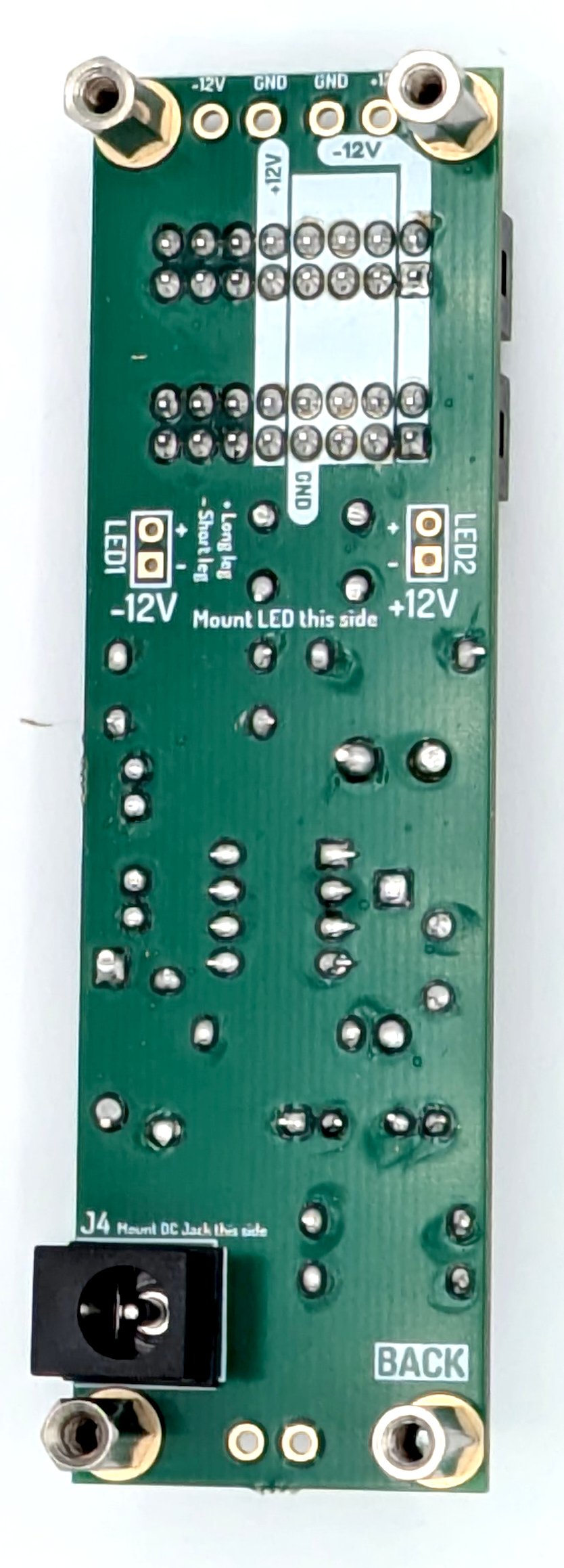
STEP 9 : PANEL ON AND LEDS
Then screw on the front panel whilst feeding through the LEDs. Note the LEDs have clear markings on the PCB to which way around they go. I like to solder them in so they poke out, or you can do it flush with the surface, it is up to you.
STEP 10 : PUT IN IC
Watch the orientation of the IC, it should be facing upwards if looking at the FRONT of the PCB in the socket. You will need to bend the pins straight, using a special tool or by bending them on a desk surface.
STEP 11 : PREFLIGHT
Follow the follwing checks to make sure that no damage could be made to the board.
- Before plugging in, put a multimeter in ohmic or "beep" mode, and test across the +12V, -12V and GND outputs and 12V inputs, this should tell you if there are shorts.
- Really inspect the board closely and use your iron to melt any pads that look a bit odd or poorly covered, you should see no gold showing through on the pad.
TROUBLESHOOTING
I highly reccomend you join the Discord server as there is plenty of help there, with forums set up per-module so you can see what other people have been struggling with.
- Look at all the solder joints. Do they look fine to you? Make sure there is no bridging between pads and there are no dry joints. When starting out this is the most common point of failure. This check can also save a component that could be damaged by a short. The pad should be fully filled with solder showing no gold.
- Check and check again that you got everything in the right orientation and the right value, especially if the diodes are reversed, nothing will power then!